← Mitsubishi Galant Engine Diagram – Know Your Car! We drive the mitsubishi triton extreme H4656 Wiring Diagram – Solve Your Electrical Mystery! Magnetek 6345 wiring diagram →
If you are searching about A detailed guide to PCB layout design - IBE Electronics you've came to the right place. We have 25 Pics about A detailed guide to PCB layout design - IBE Electronics like Practical Guidelines for High-Speed PCB Layout and Critical Component, Some LVDS PCB Layout Guidelines For Ensuring Signal, 40% OFF and also PADS Standard Layout - Mentor Graphics. Here it is:
A Detailed Guide To PCB Layout Design - IBE Electronics
 www.pcbaaa.com
A detailed guide to PCB layout design - IBE Electronics
Some LVDS PCB Layout Guidelines For Ensuring Signal Integrity | PCB
 resources.altium.com
Some LVDS PCB Layout Guidelines for Ensuring Signal Integrity | PCB ...
PCB Design Layout Guidelines For Engineers | Advanced PCB Design Blog
 resources.pcb.cadence.com
PCB Design Layout Guidelines for Engineers | Advanced PCB Design Blog ...
Some LVDS PCB Layout Guidelines For Ensuring Signal Integrity | PCB
Some LVDS PCB Layout Guidelines for Ensuring Signal Integrity | PCB ...
Practical Guidelines For High-Speed PCB Layout And Critical Component
 www.scribd.com
Practical Guidelines for High-Speed PCB Layout and Critical Component ...
Some LVDS PCB Layout Guidelines For Ensuring Signal Integrity | PCB
 resources.altium.com
Some LVDS PCB Layout Guidelines for Ensuring Signal Integrity | PCB ...
Some LVDS PCB Layout Guidelines For Ensuring Signal, 40% OFF
 www.oceanproperty.co.th
Some LVDS PCB Layout Guidelines For Ensuring Signal, 40% OFF
Some LVDS PCB Layout Guidelines For Ensuring Signal, 40% OFF
 www.oceanproperty.co.th
Some LVDS PCB Layout Guidelines For Ensuring Signal, 40% OFF
Interesting PCB Layout Design Guidelines For Signals Above 20Gbps
 www.fedevel.com
Interesting PCB Layout Design Guidelines for Signals above 20Gbps
PCB Layout Design By Siemens | PADS Professional | Cadlog
 www.cadlog.com
PCB Layout Design by Siemens | PADS Professional | Cadlog
PCB Layout Guidelines | Design Rules & Requirements | Tips
 www.wellpcb.com
PCB Layout Guidelines | Design Rules & Requirements | Tips
PCB Layout Design By Siemens | PADS Professional | Cadlog
 www.cadlog.com
PCB Layout Design by Siemens | PADS Professional | Cadlog
Some LVDS PCB Layout Guidelines For Ensuring Signal, 40% OFF
 www.oceanproperty.co.th
Some LVDS PCB Layout Guidelines For Ensuring Signal, 40% OFF
PCB Layout Services – Electronics Engineering Design Services
 www.microelectronicos.net
PCB Layout Services – Electronics Engineering Design Services
BASIC PCB Design Rules – Layout
 epci.eu
BASIC PCB Design Rules – Layout
How To Design PCB Layout? - Guidelines, Advantages And Disadvantages
 compuinfohub.blogspot.com
How to Design PCB Layout? - Guidelines, Advantages and Disadvantages ...
Top PCB Design Guidelines Every PCB Designer Needs To Know | Altium
 www.pinterest.co.uk
Top PCB Design Guidelines Every PCB Designer Needs to Know | Altium ...
LVDS: High Speed LVDS PCB Design Guidelines | MADPCB
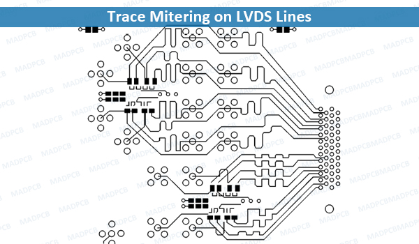 madpcb.com
LVDS: High Speed LVDS PCB Design Guidelines | MADPCB
Top 5 PCB Design Rules You Need To Know | PCB Design Blog | Altium
 resources.altium.com
Top 5 PCB Design Rules You Need to Know | PCB Design Blog | Altium
PCB Layout Guidelines.pdf
 www.slideshare.net
PCB Layout guidelines.pdf
Pcb Layout Guidelines For Design By PCBCART - Issuu
 issuu.com
Pcb layout guidelines for design by PCBCART - Issuu
PADS Standard Layout - Mentor Graphics
 www.pads.com
PADS Standard Layout - Mentor Graphics
Layout PCB Inverter: Tips And Best Practices For Successful Design
 hillmancurtis.com
Layout PCB Inverter: Tips and Best Practices for Successful Design ...
The 13 Most Used PCB Layout Design Tools
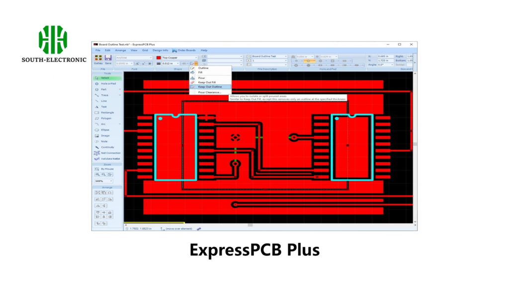 southelectronicpcb.com
The 13 Most Used PCB Layout Design Tools
Practical PCB Design Layout Rules - Leading PCB Manufacturer - Arisentec®
 arisentecpcb.com
Practical PCB design layout rules - Leading PCB Manufacturer - Arisentec®
Some lvds pcb layout guidelines for ensuring signal integrity. Top 5 pcb design rules you need to know. Interesting pcb layout design guidelines for signals above 20gbps